
Digital Logic Examples
Combinatorial Logic
We start off with a verbal description of what we want to achieve. We’ll return to the example mentioned at the end of the last activity, a three-switch arrangement in the interlocks for a high power laser.

The photograph shows a laboratory used for preparation of thin films of novel electronic materials. The big grey box at the back is a laser emitting 248m radiation in 20ns pulses with an energy up to 1 J in a beam with an area of 2 cm2. That’s an energy density of 5 kJ m2 and a power density of power of 2.5 x 10¹¹ W m-2. This is UV radiation – sufficient give you skin damage like severe sunburn.
A three switch-system could be implemented to protect personnel from the laser beam, with a switch S1 on the door to the lab, a switch S2 on the plastic covers you can see over the beam path, and an over-ride S3 switch for all these interlocks which a maintenance technician might make use of. To fire the beam in normal use, we want S1 and S2 to be closed and S3 open. We choose this way round because switches activated by doors generally close (complete an electrical circuit) when a door is closed. When the switch is closed, the logic level is low (see step 3.4, Digital Electronics), so this is an Active-LOW system.
Our implementation plan starts with a statement of the physical system.
“The laser can be fired if, and only if, S1 is closed and S2 is closed and S3 is open”.
We can draw a representation of our digital network that is entirely symbolic, containing no details at all, as in Figure 1. S1, S2 and S3 are binary variables representing the state of the switches and L is a binary variable representing the output of the network.
 Figure 1: Logic network for laser safety system (Click to expand)
Logic gates
We need to produce the appropriate output from the possible combinations of inputs, which we achieve using logic gates. Table 1 shows the symbols for eight logic gates, some or all of which you may recognise.
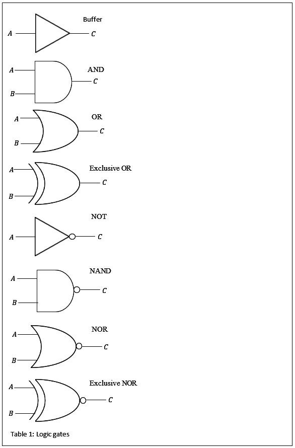 Table 1: Logic Gates (Click to expand)
Table 2 below defines each gate in words and then in Boolean logic. You might be used to drawing truth tables for the gates but in complex systems this becomes very ungainly so we’ll use the Boolean logic representation here.
| Gate | Description | Boolean representation |
|---|---|---|
| Buffer | Output is true only if the input is true | (C=A) |
| AND | Output is true if, and only if, all inputs are true | (C=A∙B) |
| OR | Output is true if, and only if, at least one input is true | (C=A+B) |
| Exclusive OR | Output is true, if and only if, one or other of the inputs is true, but not if both are true | (C=A⊕B) |
| NOT | Output is true only if the input is false | (C=frac{}{A}) |
| NAND | Output is false if and only if all inputs are true | (C=frac{}{(A∙B)}) |
| NOR | Output is false if and only if at least one input is true | (C=frac{}{(A+B)}) |
| Exclusive NOR | Output is true when both inputs are false or both inputs are true | (C=frac{}{(A⊕B)}) |
Table 2: Definitions of logic gates.
Now we can state our implementation plan in the language of Boolean logic. Remember that active-LOW means that the active state of a switch is a 0 or FALSE status. We can say
“The laser can be fired if, and only if, S1 is FALSE AND S2 is FALSE AND S3 is TRUE”.
If “the laser can be fired” then we want L to be TRUE if, and only if, S1 is FALSE AND S2 is FALSE AND S3 is TRUE”
Note that we can’t have any combination of two FALSE and one TRUE inputs, we have to be specific.
If we start from left to right in our design statement, we first require both S1 AND S2 to be FALSE. The Boolean equation for an intermediate output C would be
[C:=frac{ }{S1}.frac{ }{S2}]
If you know “de Morgan’s law” for simplifying Boolean expressions, then you know that
[C:=frac{ }{S1}.frac{ }{S2}=frac{ }{S1:+:S2}]
From Table 2 we can see we need a NOR gate. If you didn’t know this theorem then you could work out the same answer from expressing the definition of the NOR gate in a different way; the NOR gate gives a TRUE output only when none of the inputs are TRUE.
A third way of arriving at this answer is to draw a truth table for each gate. We’ll have a look at these in the quiz that follows later this week.
In any case, our next step is to combine with C with S3
[L:=:Ccdot S3]
We can achieve this with an AND gate. So now we can draw a circuit diagram for our logic network, as shown in Figure 2.
 Figure 2: Logic network for laser safety (Click to expand)
There may be are other ways to achieve the same output. As a designer, the simplest is often best, because there is less to go wrong.
Why did we provide a sub-title Combinatorial Logic in this section? The answer is that in this example we don’t have to worry about the order in which the switches are opened or closed. We are only worried about the present state of the system. We do not care about the past.
Sequential Logic
In Sequential Logic the outputs are determined by the sequence of inputs that lead to the present state of the system. We need sequential logic when the order of events, the way in which we arrived at our present state, is important.
There are two types of sequential logic, synchronous which means the outputs update only on the receipt of pulses from a clock signal, and asynchronous which means the outputs update on receipt of any input signals.
If we wanted to make a new design feature, for example that must be closed first, then we would need asynchronous logic.
However, even if we don’t mind about the order of events there could be a reason to use synchronous logic. We said in a previous article that digital systems are resistant to noise because they rely on transitions, but we have been considering HIGH and LOW levels in our circuits.
To introduce sequential logic, we’ll look at the type-D flip-flop. This component copies its input to its output when instructed to do so by a clock signal. Figure 3. gives an idea of how it works.
 Figure 3: Digital waveforms for the door sensor output, clock and type-D flip-flop (Click to expand)
In Figure 3 the door is initially open, so S1= HIGH. When the door is closed and S1= LOW the output Q of the flip-flop latches to the new input value only after a clock (CLK) pulse has arrived. The trigger for change is one of the edges of the pulse, a type-D flip-flop can be positive edge-triggered or negative-edge triggered. Figure 4. shows the circuit symbol for a positive edge-triggered device. The input is generally labelled D. An inverted output Q– is provided in addition to the main output Q. The output of the type-D flip-flop copies the input and so holds, or remembers, the logic level. The output Q will replace the S1 input in Figures 1 and 2.
 Figure 4: Type-D flip-flop (Click to expand)
Imagine there is some noise in the circuits providing power to S1. If we are unlucky, the noise will be large enough to make the system change state. But we will only react to a change of state if there is also a clock pulse. Note in Figure 3 that the clock signal has a low duty cycle – it is HIGH for less time than it is LOW. If the clock pulse is sharp enough, the noise will be missed. Our system is more robust with synchronous logic.
There are other ways to deal with noise in gates, but these are beyond the scope of this course.
Electrical Engineering: Sensing, Powering and Controlling


Electrical Engineering: Sensing, Powering and Controlling
Reach your personal and professional goals
Unlock access to hundreds of expert online courses and degrees from top universities and educators to gain accredited qualifications and professional CV-building certificates.
Join over 18 million learners to launch, switch or build upon your career, all at your own pace, across a wide range of topic areas.