
Superconducting systems
In an earlier Step, we visited the laboratory of Professor Yasunobu Nakamura at the University of Tokyo, and learned about using electric charge and magnetic flux as our qubit state variable. In this video, we continue that visit and learn more about how those experiments are conducted.
Experiments in a refrigerator
The large can behind Professor Nakamura in the video is a dilution refrigerator, which has several stages that are each progressively cooler. Inside the dil fridge is a large rig that passes through the stages, like this:
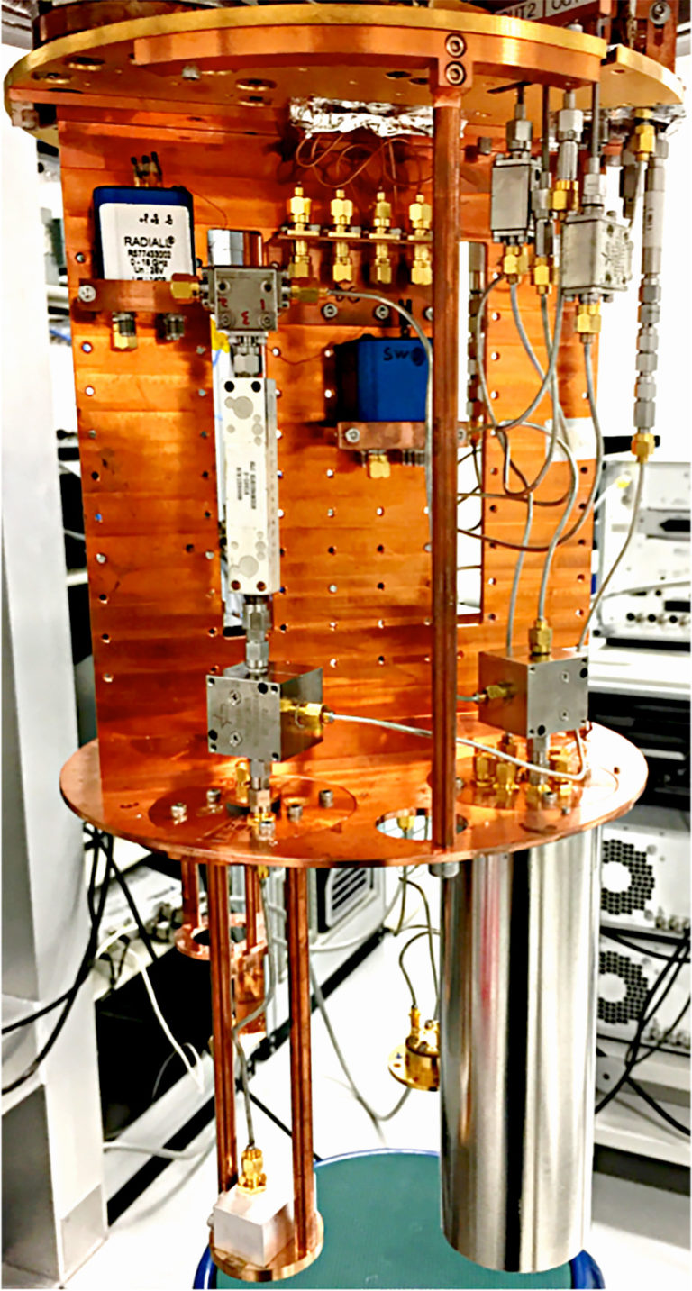 Figure provided by courtesy of Prof. Yasunobu Nakamura.
The figure below shows how a qubit is controlled from the outside (as we saw in the video), with different parts of the circuit at different temperatures: room temperature (“RT” in the figure), 4 Kelvin, then 10 millkelvin – 1/100th of a degree above absolute zero! (Quantum dot experiments use a similar physical setup to cool their chips.)
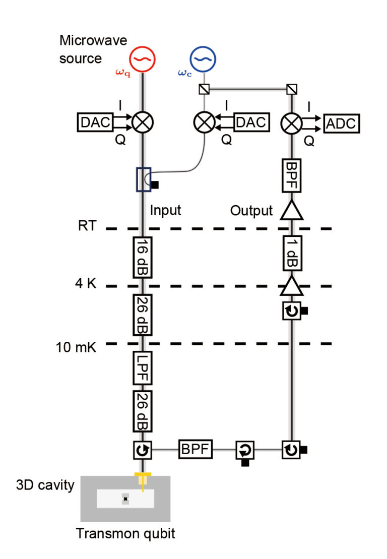 Figure provided by courtesy of Prof. Yasunobu Nakamura.
At the bottom stage is a block of aluminum with two halves, each with a single connector for a coaxial cable. Mounted inside is a small, rectangular chip, a few millimeters in size. This chip has a single transmon qubit that is about one micron in size, as you can see in the figure below. The Josephson junction itself is small, but including the resonators necessary to shield and control the qubit, the overall size is nearly a millimeter.
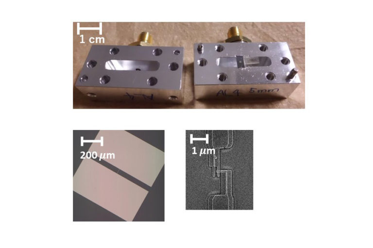 Figure provided by courtesy of Prof. Yasunobu Nakamura.
Future designs
The figure below is a computer rendering of a new chip design. The qubits are the yellow concentric circles at each lattice site. The inner and outer rings are bridged with a Josephson junction to form a transmon qubit. The qubit has four arms to interact with its neighbors. The qubits are controlled from below the chip, as you can see in the cutaway.
The four meander lines are readout resonators, used to measure the state of a qubit. Four qubits share one readout connection which is connected to a coaxial cable beneath the chip (not shown).
The small white holes that pass through the chip connect the red sheets on the top and bottom, called ground planes, to stabilize the voltage used as ground. The yellow control lines from the bottom are coaxial cables, shown in cutaway, used to execute one-qubit rotations and couple two neighboring qubits, so that we can perform two-qubit gates like CNOT.
The picture is just a schematic and not the final design, but it gives you the idea of what it takes to create a system, rather than just a single qubit in an experiment. If this design is successful, Professor Nakamura’s team will be able to build chips with tens or hundreds of qubits on them. Designs like this may be able to run surface code error correction, which we will introduce in the next Activity.
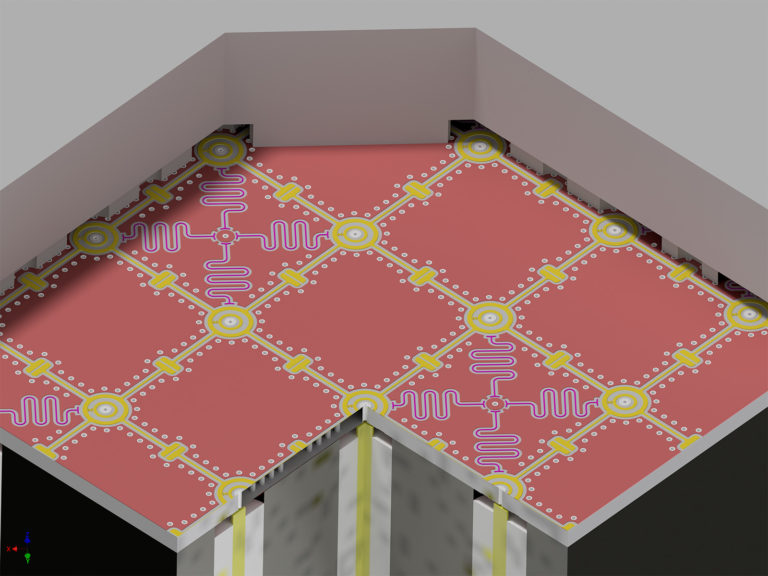 Figure provided by courtesy of Prof. Yasunobu Nakamura.
Superconducting qubits, especially transmons, are large size compared to transistors. We won’t be able to put many qubits into a single chip, and entangling two superconducting qubits in separate chips is one of the major outstanding challenges.
超電導システム
これまでの講義では東京大学の中村泰信教授の研究室を訪れ電荷と磁束を量子ビットの状態変数として扱ったシステムについて学習しました。この動画ではさらに掘り下げ、そこで行われていた実験が実際にどのように繋がってくるかを学習します。
冷却装置の中での実験
中村教授の研究室で使われている巨大な装置は希釈冷凍法と呼ばれる極低温領域での冷却法により冷却します。装置の中には大きな円材が写真のように配置されています。
図は中村泰信教授により提供されました。
下の図は各量子回路と温度帯毎にどのように量子ビットを制御するかを表しています。上から室温(RT)、4ケルビン、そして10ミリケルビン(絶対零度の-1/100の温度)という順番になっています(量子ドットの実験も似たような設計になっています)。
図は中村泰信教授により提供されました。
最下層には半分に分かれたアルミニウムの塊がありそれぞれケーブルのコネクターとセットになっています。内部には小さな長方形のチップが埋め込まれています。この場合では約1mm程のtransmon量子ビットが使われています(transmon量子ビットに使われているジョセフソン接合が実際に占める面積はとても小さいです)。
図は中村泰信教授により提供されました。
今後の動向
下の図は新型チップの図です。量子ビットは黄色の格子点に配置されます。量子ビットの内側のリングと外側のリングはジョセフソン接合によりtransmon量子ビットと呼ばれる超電導量子ビットが作り出されます。各量子ビットには隣接された量子ビットと相互作用するために4本の腕上の線があります。
そして4本セットになっている蛇上に伸びた線は量子ビットの測定に用いられています。図上では記載されていない部分もありますが、1セット毎に4つの量子ビットの測定に用いられます。
黄色の格子点上にある極小の小さな孔は赤い基盤とその上下に存在する地板を接続し、電圧を安定させるために使われます。図の下から伸びる黄色い線は単一回転ゲートやCNOTゲートなどの隣接された量子ビットとの処理に用いられます。
図はイメージであり実際のデザインではないですが、実験の説明だけではなく実際に図を見て解説する事でより理解が深める事ができます。設計が完成すれば、中村教授の研究グループは数十や数百の量子ビットを実装することが可能になります。このような設計は量子エラー訂正機能を走らせる事も可能になるでしょう。
図は中村泰信教授により提供されました。
超伝導量子ビット、特にトランスレノンは、トランジスタに比べてサイズが大きいです。私達は単一のチップに多くの量子ビットを入れることはできず、2つの超伝導量子ビットを別々のチップに絡ませることは、大きな課題の一つです。


Reach your personal and professional goals
Unlock access to hundreds of expert online courses and degrees from top universities and educators to gain accredited qualifications and professional CV-building certificates.
Join over 18 million learners to launch, switch or build upon your career, all at your own pace, across a wide range of topic areas.